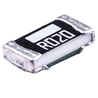
长电CJ2301 mos管,SOT-23晶体管
2022-11-14 09:16:48
毛重:0.000011KG
分类:MOSFET
品牌:JSCJ(长晶科技)
封装:SOT-23极性
Polarity:P
V(BR)DSS(Max)(V):-20V
漏极电流ID:-2.3A
漏源导通电阻RDS(on):0.112Ω
最大耗散功率PD:0.4W
漏源电压VDS:-0.4V
原厂料号:CJ2301
采购链接:https://bomyg.com/goodsInfo/411028.html
图片展示:

Encapsulate MOSFETS
BSS84 P-CHANNEL MOSFET
V(BR)DSS | RDS(on)MAX | ID |
-50V | 8Ω@-10V | -0.13A |
10Ω@-5V |
DESCRIPTION
These miniature surface mount MOSFETs reduce power loss conserve energy, making this device ideal for use in small power management circuitry.
FEATURE
z Energy Efficient z Low Threshold Voltage z High-speed Switching z Miniature Surface Mount Package Saves Board Space
APPLICATION MAXIMUM RATINGS (Ta=25℃ unless otherwise noted)
z DC−DC converters,load switching, power management in portable and battery−powered products such as computers, printers, cellular and cordless telephones.
MARKING Equivalent Circuit
Parameter | Symbol | Value | Unit |
Drain-Source Voltage | VDS | -50 | V |
Gate-Source Voltage | VGS | ±20 | V |
Continuous Drain Current | ID | -0.13 | A |
Pulsed Drain Current (note 1) @tp <10 μs | IDM | -0.52 | A |
Power Dissipation | PD | 225 | mW |
Thermal Resistance from Junction to Ambient (note 2) | RθJA | 556 | ℃/W |
Operation Junction and Storage Temperature Range | TJ,TSTG | -55~+150 | ℃ |
Maximum Lead Temperature for Soldering Purposes , Duration for 5 Seconds | TL | 260 | ℃ |
1
MOSFET ELECTRICAL CHARACTERISTICS
T =25a ℃ unless otherwise specified
Parameter | Symbol | Test Condition | Min | Typ | Max | Unit |
STATIC CHARACTERISTICS | ||||||
Drain-source breakdown voltage | V (BR)DSS | VGS = 0V, ID =-250µA | -50 | V | ||
Zero gate voltage drain current | IDSS | VDS =-50V,VGS = 0V | -15 | µA | ||
VDS =-25V,VGS = 0V | -0.1 | µA | ||||
Gate-body leakage current | IGSS | VGS =±20V, VDS = 0V | ±5 | µA | ||
Gate threshold voltage (note 3) | VGS(th) | VDS =VGS, ID =-250µA | -0.9 | -1.6 | -2 | V |
Drain-source on-resistance (note 3) | RDS(on) | VGS =-5V, ID =-0.1A | 5.8 | 10 | Ω | |
VGS =-10V, ID =-0.1A | 4.5 | 8 | Ω | |||
Forward transconductance (note 1) | gFS | VDS=-25V; ID=-100mA | 50 | mS | ||
DYNAMIC CHARACTERISTICS (note 4) | ||||||
Input capacitance | Ciss | VDS =5V,VGS =0V,f =1MHz | 30 | pF | ||
Output capacitance | Coss | 10 | pF | |||
Reverse transfer capacitance | Crss | 5 | pF | |||
SWITCHING CHARACTERISTICS (note 4) | ||||||
Turn-on delay time | td(on) | VDD=-15V, RL=50Ω, ID =-2.5A | 2.5 | ns | ||
Turn-on rise time | tr | 1 | ns | |||
Turn-off delay time | td(off) | 16 | ns | |||
Turn-off fall time | tf | 8 | ns | |||
SOURCE−DRAIN DIODE CHARACTERISTICS | ||||||
Continuous Current | IS | -0.13 | A | |||
Pulsed Current | ISM | -0.52 | A | |||
Diode forward voltage (note 3) | VSD | IS=-0.13A, VGS = 0V | -2.2 | V | ||
Notes :
1. Repetitive rating : Pulse width limited by junction temperature.
2. Surface mounted on FR4 board , t≤10s.
3. Pulse Test : Pulse Width≤300µs, Duty Cycle≤2%.
4. Guaranteed by design, not subject to producting


 售前客服
售前客服